SPI Protocol
Serial Peripheral Interface
Preface
More
and more serial bus systems are preferred instead of a parallel bus, because of
the simpler wiring. As the efficiency of serial buses increases, the speed advantage
of the parallel data transmission gets less important. The clock frequencies of
SPI devices can go up to some Megahertz and more. There are a lot of
application where a serial transmission is perfectly sufficient. The usage of
SPI is not limited to the measuring area, also in the audio field this type of
transmission is used.
The
SPI (this name was created by Motorola) is also known as Microwire,
trade mark of National Semiconductor. Both have the same functionality. There
are also the extensions QSPI (Queued Serial Peripheral Interface) and MicrowirePLUS.
The
popularity of other serial bus system like I2C, CAN bus or USB
shows, that serial busses get used more and more.
Synchronous Interfaces
Synchronous
interfaces are characterized by the presence of a dedicated receive/transmit
clock signal. A "Master" device usually outputs a clock signal that
is received by all "Slave" devices to receive and transmit data in
synch. The advantage: Each device works with the transmit/receive clock of the
master independent of any oscillator variations of each individual device; so
these interfaces are very suitable for use with cheap oscillators that have
large frequency variations
Examples of synchronous interfaces are: SPI (Serial Peripheral Interface),
developed by Motorola, MICROWIRE developed by National Semiconductor, I2C
(Inter Integrated Circuit) developed by Philips/Signetics,
and USART (Universal Synchronous & Asynchronous Receiver Transmitter) - as
the name suggests a USART can either be used in a synchronous or asynchronous
mode, so it falls into both categories.
Synchronous interfaces were designed mainly to connect peripheral devices on
the same circuit board, like external EEPROMS, A/D converters, display drivers
and sensors to microcontrollers. They are only suitable to bridge relatively
short distances (< 1 meter).
The
different Peripheral Types
The
question is of course, which peripheral types exist and which can be connected
to the host processor. Peripheral types can be subdivided into the following
categories:
·
Converters (ADC and DAC)
·
Memories (EEPROM and FLASH)
·
Real Time Clocks (RTC)
·
Sensors (temperature, pressure)
·
Others (signalmixer, potentiometer, LCD controller,
UART, CAN controller, USB controller, amplifier)
In
the three categories converters, memories and RTCs,
there is a great variety of component. Devices belonging to the last both
groups are more rarely.
There
are lots of converters with different resolutions, clock frequencies and number
of channels to choose from. 8, 10, 12 up to 24Bit with clock frequencies from
30ksps up to 600ksps.
Memory
devices are mostly EEPROM variants. There are also a few SPI flash memories.
Capacities range from a couple of bits up to 64KBit. Clock frequencies up to
3MHz. Serial EEPROMS SPI are available for different supply voltages (2.7V to
5V) allowing their use in low-voltage applications. The data retention time
duration from 10 years to 100 years. The permitted number of write accesses is
1 million cycles for most components. By cascading memory devices any number of
bits/word can be obtained.
RTCs are ideally suited for serial
communication because only small amounts of data have to be transferred. There
is also a great variety of RTCs with supply voltages
from 2.0V. In addition to the standard functions of a "normal" clock,
some RTCs offer an alarm function, non-volatile RAM
etc. Most RTCs come from DALLAS and EPSON.
The
group of the sensors is yet weakly represented. Only a temperature and a
pressure sensor could be found.
CAN
and USB controllers with SPI make it easier to use these protocols on a micro
controller and inerfacing a LCD via SPI saves the
troublesome parallel wiring.
Synchronous Microcontroller
Communication Interfaces: SPI, Microwire
At a higher level
SPI
does not have an acknowledgement mechanism to confirm receipt of data. In fact,
without a communication protocol, the SPI master has no knowledge of whether a
slave even exists. SPI also offers no flow control. If you need hardware flow
control, you might need to do something outside of SPI.
Slaves
can be thought of as input/output devices of the master. SPI does not specify a
particular higher-level protocol for master-slave dialog. In some applications,
a higher-level protocol is not needed and only raw data are exchanged. An
example of this is an interface to a simple codec. In other applications, a
higher-level protocol, such as a command-response protocol, may be necessary.
Note that the master must initiate the frames for both its command and the
slave's response.
Both
SPI and I2C offer good support for communication with low-speed devices,
but SPI is better suited to applications in which devices transfer data
streams.
SPI's full duplex communication capability
and data rates (ranging up to several megabits per second) make it, in most
cases, extremely simple and efficient for single master, single slave
applications. On the other hand, it can be troublesome to implement for more
than one slave, due to its lack of built-in addressing; and the complexity only
grows as the number of slaves increases.
Far
from being just a dumb "byte port," SPI is often an elegant solution
for modest communication needs. It can also serve as a platform on which to
create higher-level protocols.
The
Principle
In
the standard configuration for a slave device (see illustration 1), two control
and two data lines are used. The data output SDO serves on the one hand the
reading back of data, offers however also the possibility to cascade several
devices. The data output of the preceding device then forms the data input for
the next IC.
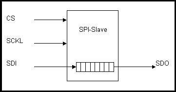
Illustration 1: SPI
slave
There
is a MASTER and a SLAVE mode. The MASTER device provides the clock signal and
determines the state of the chip select lines, i.e. it activates the SLAVE it
wants to communicate with. CS and SCKL are therefore outputs.
The
SLAVE device receives the clock and chip select from the MASTER, CS and SCKL
are therefore inputs.
This
means there is one master, while the number of slaves is only limited by the
number of chip selects.
A
SPI device can be a simple shift register up to an independent subsystem. The
basic principle of a shift register is always present. Command codes as well as
data values are serially transferred, pumped into a shift register and are then
internally available for parallel processing. Here we already see an important
point, that must be considered in the philosophy of SPI bus systems: The length
of the shift registers is not fixed, but can differ from device to device.
Normally the shift registers are 8Bit or integral multiples of it. Of course
there also exist shift registers with an odd number of bits. For example two
cascaded 9Bit EEPROMs can store 18Bit data.
If
a SPI device is not selected, its data output goes into a high-impedance state
(hi-Z), so that it does not interfere with the currently activated devices.
When cascading several SPI devices, they are treated as one slave and therefore
connected to the same chip select.
Thus
there are two meaningful types of connection of master and slave devices.
illustration 2 shows the type of connection for cascading several devices.
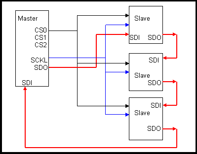
Illustration 2:
Cascading several SPI devices
In
illustration 2 the cascaded devices are evidently looked at as one larger
device and receive therefore the same chip select. The data output of the
preceding device is tied to the data input of the next, thus forming a wider
shift register.
Both
SPI and Microwire are full-duplex, (3+n)-wire serial
busses. (n= # of slaves). If independent slaves are to be connected to a master
an other bus structure has to be chosen, as shown in illustration 3. Here, the
clock and the SDI data lines are brought to each slave. Also the SDO data lines
are tied together and led back to the master. Only the chip selects are
separately brought to each SPI device.
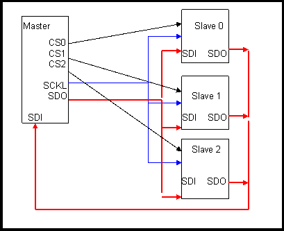
Illustration 3:
Master with independent slaves
Last
not least both types may be combined.
The
4 pins of the SPI interface are as follows:
- SCK (Serial
Data Clock): Data is shifted/latched on the rising or falling
edge of SCK.
- MOSI (Master
Output/Slave Input): Data is transmitted out of this pin if
the chip is a Master and into this pin if the chip is a Slave.
- MISO (Master
Input/Slave Output): Data is received into this pin if the
chip is a Master and transmitted out of this pin if the chip is a
Slave.
- /CS (Chip
Select, active low): Tells the peripheral that a transfer is about to
begin.
It
is also possible to connect two micro controllers via SPI. For such a network,
two protocol variants are possible. In the first, there is only one master and
several slaves and in the second, each micro controller can take the role of
the master. For the selection of slaves again two versions would be possible
but only one variant is supported by hardware. The hardware supported variant
is with the chip selects, while in the other the selection of the slaves is
done by means of an ID packed into the frames. The assignment of the IDs is
done by software. Only the selected slave drives its output, all other slaves
are in high-impedancd state. The output remains
active as long as the slave is selected by its address.
The
first variant, named single-master protocol, resembles the normal master-slave
communication. The micro controller configured as a slave behaves like a normal
peripheral device.
The
second possibility works with several masters and is therefore named
multi-master protocol. Each micro processor has the possibility to take the
roll of the master and to address another micro processor. One controller must
permanently provide a clock signal. The MC68HC11 provides a harware
error recognition, useful in multiple-master systems. There are two SPI system
errors. The first occurs if several SPI devices want to become master at the
same time. The other is a collision error that occurs for example when SPI
devices work with with different polarities. More
details can be found in the MC68HC11 manual.
Data
and Control Lines of the SPI
The
SPI requires two control lines (CS and SCLK) and two data lines (SDI and SDO). Motorola
names these lines MOSI (Master-Out-Slave-In) and MISO (Master-In-Slave-Out).
The chip select line is named SS (Slave-Select).
With
CS (Chip-Select) the corresponding peripheral device is selected. This pin is
mostly active-low. In the unselected state the SDO lines are hi-Z and therefore
inactive. The master decides with which peripheral device it wants to
communicate. The clock line SCLK is brought to the device whether it is
selected or not. The clock serves as synchronization of the data communication.
The
majority of SPI devices provide these four lines. Sometimes it happens that SDI
and SDO are multiplexed, for example in the temperature sensor LM74 from
National Semiconductor, or that one of these lines is missing. A peripheral
device which must or can not be configured, requires no input line, only a data
output. As soon as it gets selected it starts sending data. In some ADCs
therefore the SDI line is missing (e.g. MCCP3001 from Microchip).
There
are also devices that have no data output. For example LCD controllers (e.g.
COP472-3 from National Semiconductor), which can be configured, but cannot send
data or status messages.
SPI
Configuration
Because
there is no official specification, what exactly SPI is and what not, it is
necessary to consult the data sheets of the components one wants to use.
Important are the permitted clock frequencies and the type of valid
transitions.
SPI
uses a couple parameters called clock polarity (CPOL) and clock phase (CPHA) to
determine when data is valid with respect to the clock signal. These must be
set on the Master and all the Slaves in order for communication to work. CPOL
determines whether the leading edge is defined to be the rising or falling edge
of the clock (and vice versa for the trailing edge). CPHA determines whether
the leading edge is used for setup or sample (and vice versa for the trailing
edge). The following table summarizes the various settings:
|
CPOL |
CPHA |
Transfer |
|
0 |
0 |
SCK rising-edge transfer. |
|
1 |
0 |
SCK falling-edge transfer. |
|
0 |
1 |
SCK falling-edge transfer. |
|
1 |
1 |
SCK rising-edge transfer. |
The
following two waveform diagrams illustrates how these modes work:
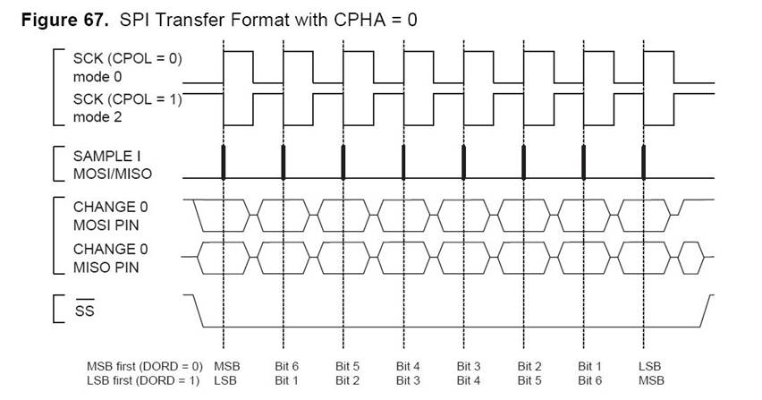
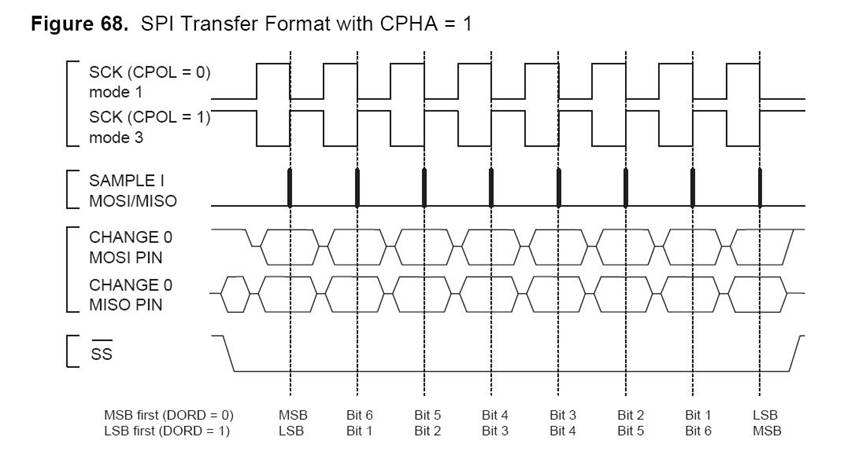
In
these examples note that either the MSB or the LSB can be sent first depending
on how the SPI hardware is configured.
Communication
between a master and slave occurs as follows:
- Master pulls
low the slave select line of the desired slave device. This indicates to
each device to prepare
for communication.
- The Master
generates the clock signal according to its SPI mode. Both Master and
Slave transmit one bit per clock cycle.
- After a byte
has been sent the Master pulls the slave select line high.
What
has been described here is all that the SPI protocol provides. There are no
handshaking or acknowledgement or any advanced communication standards
associated with it so those would have to be implemented on top of this layer
if needed. SPI is a great little protocol for situations that require simple
communication between two hosts.
Why
would you want 4 different settings? Two of the four settings allow the SPI
interface to talk to different flavors of Microwire
devices and vice versa.
Many
early SPI devices implemented only SPI mode 0 that does the opposite of Microwire, namely shift data out on the rising edge and in
on the falling. Therefore Microwire/Plus was created
that allows selecting an alternate shift clock via the SKSEL (shift clock
select) bit. Nowadays Microwire/Plus with alternate
shift clock is compatible to SPI mode 0 and Microwire
with standard shift clock is compatible with SPI mode 1.
Both
Microwire and SPI do not explicitly define any
maximum data rates. Different peripherals on the market each have their own
maximum speed limit - most of them in the several Mbit
range. There is no means of slaves to slow the master down and also no
acknowledgement on received data, like with I2C. To accommodate a wide range of
SPI/Microwire speeds, microcontrollers usually
feature a programmable shift clock divider.
Synchronous Microcontroller Communication
Interfaces: SPI and Microwire versus I2C
Microwire and SPI versus I2C
Both
SPI and I2C provide good support for communication with slow
peripheral devices that are accessed intermittently. EEPROMs
and real-time clocks are examples of such devices. But SPI is better suited
than I2C for applications that are naturally thought of as data
streams (as opposed to reading and writing addressed locations in a slave
device). An example of a "stream" application is data communication
between microprocessors or digital signal processors. Another is data transfer
from analog-to-digital converters.
SPI
is a close cousin of the older Microwire. Both
interfaces are very simple and basically consist only of an 8-bit serial shift
register and (for master devices) a programmable shift clock. There is no means
of addressing devices. SPI can also achieve significantly higher data rates
than I2C. SPI-compatible interfaces often range into the tens of
megahertz. Typical applications consist of one master device (usually a
microcontroller) and one or multiple slave devices (usually peripheral
functions, like A/D, EEPROM, display drivers, etc.). SPI really gains
efficiency in applications that take advantage of its duplex capability, such
as the communication between a "codec" (coder-decoder) and a digital
signal processor, which consists of simultaneously sending samples in and out.
SPI
devices communicate using a master-slave relationship. Due to its lack of
built-in device addressing, SPI requires more effort and more hardware
resources than I2C when more than one slave is involved. But SPI
tends to be simpler and more efficient than I2C in point-to-point
(single master, single slave) applications for the very same reason; the lack
of device addressing means less overhead.
I2C
is quite a bit more complex than SPI and Microwire,
which results in a larger silicon area and therefore slightly more expensive
devices. In addition Philips is collecting licensing fees for I2C
implementations from competitors, adding to the cost of I2C devices.
Connecting
External Peripherals
There
is a minimum of 3 connections for SPI and Microwire:
serial clock, serial data out and serial data in. Therefore you'll see those
interfaces sometimes referred to as 3-wire interfaces. The interconnected
devices need to also share the same Vcc and GND of
course and in the case of multiple connected devices you need one chip select
for each connected slave device (for just one slave, the slave's chip select
can be enabled all the time – not recommended, but possible).
If
you want to connect N devices to your microcontroller with Microwire
or SPI you need to sacrifice 3+N pins to do the job. This is an area where I2C
has an advantage. I2C features a 7-bit address as part of the
protocol. As such I2C can address up to 128 devices on the bus
without the need for dedicated chip select signals.
The
Need For Speed
Microwire and SPI shine when
it comes to speed. I2C was initially specified at a maximum speed of
100kbits/sec. This was later increased to 400kbits/sec and lately some devices
started to show up that boast 1Mbits/sec. This still pales in comparison to Microwire and SPI speeds. SPI has the edge over Microwire, due to the availability of higher speed
peripheral devices. Today's serial EEPROM for example support up to 3MBits/s
for Microwire and up to 10Mbits/sec for SPI. But even
the slowest Microwire and SPI peripherals still beat
the typical 100 or 400kbit/s I2C speeds.
Increasing the speed gap is the fact that SPI and Microwire
have full–duplex capability (can receive and send data at the same time), while
I2C, due to its two-wire nature (one clock, one data) can only
communicate half-duplex.
Why can speed be important? Current consumption for one - many microcontroller
applications spend most of their time in power save modes and only short
periods of time in "normal" operating mode. The faster a read or
write operation to a peripheral can be completed, the shorter the time the
controller needs to be active. This is especially true for access to large
external EEPROM memories.
Multi-Master
Systems
I2C
offers better support for multi-master systems. The interface has built in
arbitration to detect multiple devices sending on the bus at the same time and
to give priority to the one that first sends a "0". Microwire would require some software implemented
handshaking via a standard I/O pin to allow for multiple master devices on the
bus. SPI has a crude way to support multi-master systems via its built in
"fault logic". It can detect requests of devices to become the master
via the dedicated SS (slave select) pin.
Noise
Immunity
One
possible disadvantage of I2C should not go unmentioned: Higher noise
sensitivity and along with it lower data integrity. I2C uses a
read/write bit which follows the initial 7 address bits to tell a peripheral
whether data should be read or written. In addition I2C is level
sensitive - in contrast to Microwire and SPI, which
are edge sensitive. This means that I2C samples data during the high
or low phase of a bit and you can easily envision that noise could flip the
read/write bit. So if you wanted to read data from your external EEPROM, but
noise turned your read bit into a write bit, your memory might get corrupted. Microwire and SPI peripherals on the other hand implement
read and write operations via explicit commands send over the bus, making
selecting the "wrong" operation less likely.
So
which synchronous interface should you give the preference?
If
you have many devices to connect and in addition have multiple microcontrollers
in your system that can act as masters, then I2C is the interface of
choice. The same holds true if you need to keep the number of interconnects,
board routing and pins required for the interface to an absolute minimum. The I2C
interface is very popular in video and audio applications, due to Philips'
(microcontroller & application specific peripheral) dominance in those
applications. If you develop such applications you might not find your desired
peripheral function with any other interface.
If your main concerns are low cost, high speed or noise immunity, either Microwire or SPI are preferable. An added advantage is that
MICROWIRE/PLUS microcontrollers can talk to SPI peripherals and SPI
microcontrollers can talk to Microwire peripherals
with minimum additional software overhead, which gives you a large selection of
available peripherals to choose from for most applications.
Catching the right bus
As
you can see, there is a multitude of serial communication buses to choose from.
(And we didn't even discuss wireless, networks, Firewire,
and USB protocols.) Your choice in a serial bus should not only meet the needs
of the product today, but also be available as well as viable for the life of
the product. I hope this has helped you decide which serial interface is proper
for your current embedded design.
|
Table 1 Protocol
comparison |
|||||||
|
Name |
Sync |
Type |
Duplex |
Max |
Max |
Max |
Pin |
|
RS-232 |
async |
peer |
full |
2 |
20(2) |
30(3) |
2(4) |
|
RS-422 |
async |
multi-drop |
half |
10(5) |
10,000 |
4,000 |
1(6) |
|
RS-485 |
async |
multi-point |
half |
32(5) |
10,000 |
4,000 |
2 |
|
I2C |
sync |
multi-master |
half |
-7 |
3,400 |
<10 |
2 |
|
SPI |
sync |
multi-master |
full |
-7 |
>1,000 |
<10 |
3+1(8) |
|
Microwire |
sync |
master/slave |
full |
-7 |
>625 |
<10 |
3+1(8) |
|
1-Wire |
async |
master/slave |
half |
-7 |
16 |
1,000 |
1s |
|
Notes |
|
|
|
|
|
|
|
|
-1 |
Not including ground. |
|
|
|
|
|
|
|
-2 |
Faster
speeds available but not specified. |
|
|
|
|||
|
-3 |
Dependent
on capacitance of the wiring. |
|
|
|
|||
|
-4 |
Software
handshaking. Hardware handshaking requires additional pins. |
|
|||||
|
-5 |
Device
count given in unit loads (UL). More devices are possible if fractional-UL
receivers/transmitters are used. |
||||||
|
-6 |
Unidirectional
communication only. Additional pins needed for each bidirectional
communication. |
||||||
|
-7 |
Limitation
based on bus capacitance and bit rate. |
|
|
|
|||
|
-8 |
Additional
pins needed for every slave if slave count is more than one. |
|
|||||
Conclusions
SPI's and Microwire's
full duplex capability and fast data rates make those interfaces very efficient
and simple for single master - single slave applications. In practical
applications, the requirement for dedicated slave select signals severely
limits the number of slave devices that can be connected to a microcontroller.
Multi-master systems significantly increase complexity and are very rarely used
with those two interfaces.
I2C's
lower speed and more complex protocol put it at a disadvantage in single
master-single slave applications. Its weakness turns into strength if a larger
number of slave devices needs to be connected or a multi-master system is
needed.
All
three interfaces have the advantage of being tolerant to large oscillator
variations, as all data transfers are synchronized to the master's shift clock.
As synchronous interfaces they are, however, limited to bridging short
distances on a single PCB or between PCBs within a smaller system. When it
comes to bridging larger distances or connecting external devices, asynchronous
interfaces play a dominant role and we will start looking at some of them in
part 3 of this series.
Boards with SPI:
" ZWERG11A
" ZWERG11plus
" IC11B
" ZWERG332
" SCOTTY332
" MEGA332
" DIL2106
" LC2194
Fonte: http://www.mct.net/faq/spi.html
Aplicações:
App Note 85: Interfacing the DS1620 to the Motorola
SPI Bus
|
|
Communication with the DS1620 digital temperature sensor IC is
achieved via a simple 3-wire interface. There are a number of differences
between this interface and the Motorola SPI interface. However, a few minor
hardware and software modifications allow the DS1620 to be effectively
incorporated into an SPI based system. |
|
This
application note is a courtesy of Michel St-Hilaire and
Marc Desjardins from XyryX Technologies,
Introduction
The
DS1620 Digital Thermometer and Thermostat provides 9-bit temperature readings which
indicate the temperature of the device. With three thermal alarm outputs, the
DS1620 can also act as a thermostat. Temperature settings and temperature
readings are all communicated to/from the DS1620 over a simple 3-wire
interface.
However,
the SPI interface found on many Motorola processors cannot directly communicate
with the 3-wire interface found on the DS1620. First, the data flow to and from
the DS1620 is multiplexed on only one pin (DQ) while SPI needs two separate
signals (MOSI, MISO).
Second,
most SPI interfaces are limited to 8-bit data transfer, complicating sending
and receiving the 9-bit temperature readings to and from the DS1620. In
addition, the DS1620's interface transfers LSB first, while SPI is an MSB-first
communication protocol.
Lastly,
the RST-bar is unlike a CS-bar (chip select) signal in that RST-bar must be
high from the beginning of a transfer (protocol) to the end of all transfer of
data (e.g. 9th bit transferred when reading temperature value).
Despite
all these constraints, a fairly simple solution can be found which allows an
SPI interface to communicate with a DS1620. This technique is described in this
application note.
SPI
Interface
The
circuit shown in Figure 1 can be used to control data flow direction with an SPI
bus interfaced to a DS1620. This circuit could be integrated into a small PAL
if desired.
The
purpose of the DIR signal is to select between sending data to or receiving
data from the DS1620. When DIR is low, the DS1620 is receiving data; if DIR is
high, data is being read by the SPI controller.
The
resistor is necessary to prevent contention between the output of the tri-state
buffer on the MOSI line and the DQ pin of the DS1620, because after a READ
command protocol has been received by the DS1620, its DQ pin changes direction
from input to output in a few hundred nanoseconds. This time is much too short
for the microprocessor controlling the DIR signal to take action.
When
connecting multiple peripherals on the same SPI bus, the MISO signal must be
tri-stated when the DS1620 is not accessed to prevent contention with the MISO
signal of other peripherals. That is why the RST-bar signal is necessary in the
logic which determines the data direction.
Note that
the SPI clock is wired directly to the CLK pin of the DS1620. The software has
to take care of the polarity and phase of the SPI clock to be compatible with
the CLK timing requirements of the DS1620.
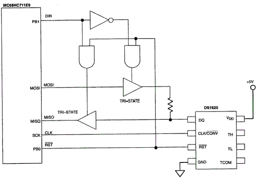
Figure 1.
SPI to DS1620 Interface Circuit
Software
for the Interface
While the
hardware for the interface is relatively straightforward, the rest of the
SPI/DS1620 interface must be handled by software. The following example shows a
way to do this in the case of reading the temperature from the DS1620. This
code fragment assumes that the DS1620 has already been initialized, that the
configuration register is set up properly, and that temperature conversions
have been initiated. See the DS1620 data sheet for details on these operating modes.
Before
accessing the DS1620, the DIR signal must be asserted low for a WRITE transfer
to occur. RST-bar must be driven high to enable the DS1620. The SPI controller
sends out the protocol (eight bits long) to the DS1620. Again, note that SPI
sends information MSB first, while the DS1620 communicates LSB first. In order
to accomplish this, a software "mirror" should be used to reverse the
bit order. An example of such a function is given by:
unsigned char mirror(unsigned char value){ unsigned char i; unsigned char value_mirrored = 0x00; for (i=0;i<=7;i++) { value_mirrored = value_mirrored | (((value>>i)&0x01)<<(7-i));}return (value_mirrored);}
With the
protocol sent, the DIR is changed from low to high (indicating now a READ
transfer) because the DS1620 is ready to send out the 9-bit value. Note that
RST-bar is still high. The SPI controller reads the first eight bits of the
9-bit value (LSB first). The software has to "mirror" the received
byte. The 9th bit (followed by seven dummy bits) is pulled out by making
another READ transfer and keeping DIR and RST-bar as they are. When the second
byte is received, the software again mirrors it and pulls RST-bar low,
terminating communication with the DS1620.
#define RST_bit 0 /* PB0 */#define RST_port PORTB#define DIR_bit 1 /* PB1 */#define DIR_port PORTB#define READ_TEMP_CMD 0xAA unsigned int read_temp(void){ unsigned char temp_value_lo; unsigned char temp_value_hi; DIR_port = DIR_port & ~(1<<DIR_bit); /* DIR = LO: WRITE mode */ RST_port = RST_port | (1<<RST_bit); /* RST = HI: DS1620 enabled */ SPDR = mirror(READ_TEMP_CMD); /* Send protocol to DS1620 */ DIR_port = DIR_port | (1<<DIR_bit); /* DIR = HI: READ mode */ while ((SPSR & (1<<SPIF_bit)) == 0); /* Wait for SPI flag = ready */ temp_value_lo = mirror(SPDR); /* Receive 8 lowest bits */ temp_value_hi = mirror(SPDR); /* Receive 8 highest bits */ RST_port = RST_port & ~(1<<RST_bit); /* RST = LO: Temp. reading done */ return ((temp_value_hi<<8)+temp_value_lo); /* Return the 9-bit value */} Interfacing
SPI Peripherals to the MAX7651 Processor
|
|
This article explains how to interface a GPIO port to an SPI
peripheral. It defines the basics of the SPI protocol, the signals and the
four transfer variations for the SCK signal. A software routine is included
to implement the SPI interface using the MAX7651, a flash programmable 12-bit
integrated data-acquisition system. |
|
When
reading a data sheet for a SPI peripheral, it is common to see a reference to
the SPI mode as CPOL = 0, CPHA = 0, etc., even though the chip itself does not
physically contain these bit definitions. Rather, the SPI interface is
"hard-wired" to send/receive data as if the CPOL and CPHA bits had
been set to 0. For example, the MAX5154 12-bit DAC uses a SPI interface with
rising-edge mid-bit data transfer. This corresponds to CPOL = 0, CPHA = 0
protocol. Because this is by far the most common SPI transfer, that is the
example code we will discuss. See the following diagram, which is from the
MAX5154 data sheet. The signal /CS is the SPI signal /SS, SCLK is SCK, and DIN
would be connected to MODI, because the peripheral is a Slave, with only an
input (no readback). This part uses 16 bits in the transfer.
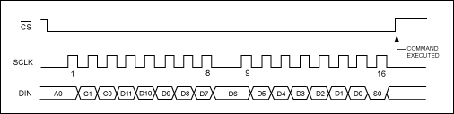
Figure 1.
Serial interface timing diagram
Code
Example: 8-Bit Data Transfer
The
following example is the most common type of SPI transfer, with CPO = 0 and
CPHA = 0. The routine does not assume anything about the clock speed of the
MAX7651, as the I/O port bits are simply "bit-banged" as fast as
possible. Data-transfer times are shown at the end of this section.
Figure 2
shows typical connections between the MAX7651/MAX7652 and an SPI peripheral.
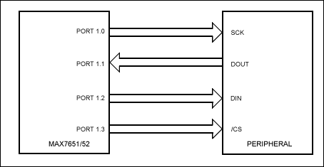
Figure 2.
General SPI connection
The
number {N} inside the comment field is the number of clock cycles to execute
the instruction.
; SPI
data transfer for 8-bit peripherals. MAX7651 is Master; peripheral is Slave.
;
; The following SPI-defined pins are used. (Some peripherals are write only,
so only 3 wires are needed.)
; SCK: The data transfer clock
; MISO: Master Input data (from peripheral), not always used
; MOSI: Master Output data (to peripheral)
; SS: Slave Select (active low)
;
|
|
SCK |
EQU |
P1.0 |
|
|
|
MISO |
EQU |
P1.1 |
|
|
|
MOSI |
EQU |
P1.2 |
|
|
|
CS |
EQU |
P1.3 |
; Use Port 1, but this is 100% arbitrary. Use any available pins. |
;
; Now we need to use some of the internal RAM in the MAX7651 as data storage.
; For speed of execution, two of these variables must be located in the
RAM area
; that allows bit addressing within the byte. In the MAX7651, the RAM space
corresponds
; to addresses 20H to 2FH. Addresses below 20H or above 2FH cannot be
bit-addressed!
|
|
SPI_In |
EQU |
20H |
;
Result of 8-bit read from Slave. |
|
|
SPI_Out |
EQU |
21H |
;
Data we wish to send to Slave. |
;
; Lastly, we need a loop counter to keep track of sending the 8 bits.
; This can be either an 'R' register (R0-R7) or
; any RAM register (doesn't have to be bit-addressable). Let's use a RAM
; register.
|
|
LOOP |
EQU |
30H |
;
Can be anywhere in the map; this is just an example. |
;
; It is assumed that when called, the chip select bit SS is already set to 1.
|
SPI_IO: |
CLR |
SCK |
; SCK starts off low. {1} |
|
|
CLR |
CS |
; Clearing CS begins the data transfer. {1} |
|
|
SETB |
MISO |
; To be used as input, must be set internally. {1} |
|
|
MOV |
LOOP,#8 |
; Eight bits to transfer. {3} |
|
XFER: |
MOV |
C,SPI_Out.7 |
; Move bit 7 into Carry (SPI is MSB first). {2} |
|
|
MOV |
MOSI,C |
; I/O port reflects the Carry bit, which is the Data bit. {2} |
|
|
SETB |
SCK |
; Generate SCK rising edge, after Data is stable. {1} |
|
|
MOV |
C,MISO |
; Read data from Slave into Carry (optional). {2} |
|
|
MOV |
SPI_In.7,C |
; Copy into the received data byte, bit-7 position. {2} |
|
|
CLR |
SCK |
; Generate SCK falling edge, after data read in. {1} |
|
|
MOV |
A,SPI_Out |
; Accumulator is temp holder for shift operation. {2} |
|
|
RL |
A |
; Rotate left (but not through Carry!). {1} |
|
|
MOV |
SPI_Out, A |
; Prepare bit 7 for next transfer to Slave. {2} |
|
|
MOV |
A,SPI_In |
; Get previous Slave read data. {2} |
|
|
RL |
A |
; Rotate left to get next bit position into proper spot. {1} |
|
|
MOV |
SPI_In,A |
; Save result. {2} |
|
|
DJNZ |
LOOP,XFER |
; Decrement LOOP. Jump if not zero to XFER. {3} |
|
; Transfer done. |
|||
|
|
SETB |
CS |
; De-assert chip select. {1} |
|
|
.END |
|
; Tell assembler code completed. |
The total
number of CPU cycles to transfer 8 bits (both read and write to Slave) is 6 + 8
23 + 1 = 191. For reading or writing only, the total is 6 + 8 18 + 1 = 151 CPU
cycles. The following table shows various transfer rates using common MAX7651
clock speeds.
Table 2. Transfer Rates
|
MAX7651 Clock Speed |
Bit Transfer Time |
Total Read/Write |
|
12MHz |
7.95us (~125KHz) |
63.6us |
|
11.0592MHz |
8.63us (~116KHz) |
69.08us |
|
4MHz |
23.88us (~41.9KHz) |
191us |
From this
table, we can see that the fastest SPI byte transfer is approximately 15.7KHz
whereas the slowest rate is 5.2KHz. This is much slower than a dedicated 1MHz
SPI hardware port! Therefore, if the MAX7651 is to be used as a Slave, then the
SPI Master must be set for the slowest bit transfer speed (125KHz) and the
MAX7651 must operate at a 12MHz clock speed.
Using the BX24 SPI Port to Interface with a MAX7219
8-Digit LED Display Driver
copyright,
Peter H Anderson, Baltimore, MD, Feb 00
Introduction
This discussion
illustrates the use of the BX24's SPI Port to interface with the MAX7219 eight
7-seg LED Driver. The advantage in using the SPI interface is that the MAX7219
may be controlled using only one (vs three) of the
precious 16 general purpose IO pins. SCK and MOSI on the BX24 SPI interface are
used and these may also be shared with other SPI devices as well.
Earlier routines
developed in Dec, '99, used three of the 16 general purpose IO terminals on the
BX24 for CLK, DAT and CS. A minor revision was made
in Feb, '00 to modify the MAX7219Init() routine to write a zero to MAX7219
register 15 (&H0F) so as to place the MAX7219 in "normal"
operation as opposed to "test" operation where all segments of all LEDs are continually turned on.
The
following routine MAX7219_1B.Bas is a rework of MAX7219_1.Bas from Dec, '99
which uses the BX24's SPI interface. Note that SCK (hole 3) on the BX24 is
connected to CLK (term 13) on the MAX7219 and MOSI (Master Out Slave In) at
hole 5 of the BX24 is connected to DIn (term 1) on
the MAX7219. One general purpose IO is used to select the specific SPI address.
A
schematic of this arrangement is included with our MAX7219 Kit.
The
software revisions are minor. In Sub Main() an SPI channel is opened using the OpenSPI() command. I happened to define this as SPI channel
2 using terminal 12 as the chip select.
Sub
Max7219Out16(ByVal X as Integer) was modified to use
the SPICmd() routine as opposed to "bit
banging" as was used in the December version. Note that the high and low
bytes of X are placed in contiguous locations beginning at the address of PutData(1) and are then output using the SPICmd()
I will
leave it for you to modify the various routines which were developed in Dec,
'99. Simply open an SPI channel in Main() and substitute this modified
implementation of Sub Max7219Out16().
' MAX7219_1B.Bas'' Illustrates the use of a MAX7219 Serially Interfaced, 8-Digit Display ' Driver. Same as MAX7219_1.Bas except uses BX24's SPI Bus.'' The only differences are that in Sub Main, an SPI Channel is opened;'' Call OpenSPI(2, SPISetUpByte, MAX7219CS) ' CS is terminal 12'' and in Sub Max7219Out16(ByVal X as Integer), the integer X is split into ' high and low bytes and output using the SPICmd()'' Example uses four MAN74 7-Segment LEDs (Common Cathode) as Digits 3, 2, ' 1 and 0.'' BX-24 MAX7219'' SCK (Hole 3) ----------- CLK (term 13)' MOSI (Hole 5) ----------- DIN (term 1)'' CS (term 12) ------------ LOAD (term 12)'' Note that the "holes" refer to the array of seven holes at the top of the ' BX24. Hole 1 is closest to terminal 24. '' In initializing the MAX7219;'' Decode Mode (Register 9) set for Code B on all digits.' Intensity (Register 10) set for 15/32' Scan Limit (Register 11) set for Digits 0, 1, 2, 3' Display Test (Register 15) set for normal operation.'' The numbers 0000 - 9999 are sequentially displayed. No sign and no zero' suppression.'' Note that in outputting the 16 bit quantity, the quantity is split into' a high and low byte and each is then output.'' This was a part of a Senior Project by Kenrick David.'' copyright, Peter H. Anderson, Baltimore, MD, Feb, '00 Const DecodeModeCode as Integer = &H900 Const IntensityCode as Integer = &Ha00 Const ScanLimitCode as Integer = &Hb00 Const TurnOnCode as Integer = &Hc00 Const DisplayTestCode as Integer = &Hf00 Const MAX7219CS as Byte = 12 ' define SPI Setup Bits Const SPI_LSB as Byte = &H20 'lsb transmitted first Const SPI_CPOL as Byte = &H08 'sck is mostly high Const SPI_CPHA as Byte = &H04 'clock phase, see atmel docs for timing Const SPI_SCK4 as Byte = &H00 'clock speed f/4 Const SPI_SCK16 as Byte = &H01 'clock speed f/16 Const SPI_SCK64 as Byte = &H02 'clock speed f/64 Const SPI_SCK128 as Byte = &H03 'clock speed f/128 Sub Main() Dim Q as IntegerDim N as Integer
Dim SPISetUpByte as Byte
Call OpenSerialPort(1, 19200) ' used for debugging
SPISetUpByte = 0 ' most sig first, 0 0 clocking, f/4 Call OpenSPI(2, SPISetUpByte, MAX7219CS) ' open an SPI channel ' using term 12 as CS Do Call Max7219Init() For N = 0 to 9999 Call Max7219PutUI(N) ' unsigned intger, no zero suppression Call Sleep(1.0) Next LoopEnd Sub Sub Max7219Init() ' initialize, Code B, 15/32 intensity, Digits 0, 1, 2, 3, Display On, ' Test Mode Off Call Max7219Out16 (DisplayTestCode) ' Normal Operation vs Test Call Max7219Out16 (DecodeModeCode OR &Hff) 'Sets Decode Mode Call Max7219Out16 (IntensityCode OR &H07) 'Sets Intensity Call Max7219Out16 (ScanLimitCode OR &H03) 'Sets Scan Limit Call Max7219Out16 (TurnOnCode OR &H01) ' Turn it on End Sub Sub Max7219PutUI(ByVal Q as Integer) ' 4 DigitsDim D as Integer
D = Q\1000Call Max7219Out16(4*256 + D) ' note 00000100 in high byte - Digit 3
Q = Q Mod 1000 D = Q\100 Call Max7219Out16(3*256 + D) ' 0000 0011 in high byte - Digit 2 Q = Q mod 100 D = Q\10 Call Max7219Out16(2*256 + D) ' Digit 1 Q = Q Mod 10 D = Q Call Max7219Out16(1*256 + D) ' Digit 0 End Sub Sub Max7219Out16(ByVal X as Integer)' shifts out 16-bit quantity, most sig bit first Dim PutData(1 to 2) as Byte, H as Byte, L as Byte Dim GetData as Byte H = CByte(X\256) ' Split into high and low bytesL = CByte(X - (CInt(H)*256))
PutData(1) = H ' and put into contiguous addresses
PutData(2) = L ' Call PutB(H) ' used for debugging ' Call PutByte(Asc(" ")) ' Call PutB(L) ' Call NewLine() Call SPICmd(2, 2, PutData(1), 0, GetData) ' Output two bytes beginning ' at location of PutData(1)End Sub References: · http://dbserv.maxim-ic.com/appnotes.cfm?appnote_number=802
- http://www.epanorama.net/links/serialbus.html
- http://www.ucpros.com/work%20samples/Microcontroller%20Communication%20Interfaces%202.htm
· http://www.phanderson.com/basicx/max7219_spi.html
· http://dbserv.maxim-ic.com/appnotes.cfm?appnote_number=427
- http://www.embedded.com/story/OEG20020528S0057
- http://www.wfe.com.tw/chinese/pro/microchip/eeprom/main4.htm
Related Links:
·
An Introduction to
Fairchild's 'SPI' Interface EEPROMs -
Application note in PDF format.
·
App Note 085:
Interfacing the DS1620 to the Motorola SPI Bus - The DS1620
Digital Thermometer and Thermostat provides 9-bit temperature readings which
indicate the temperature of the device. SPI interface found on many Motorola
processors cannot directly communicate with the 3-wire interface found on the
DS1620.
·
D.4
Serial Peripheral Interface - Some information on SPI bus implementatin
on one microcontroller board and and netwoking with SPI bus.
·
Interfacing
SPI Peripherals to the MAX7651 Processor - This document has
a good description of operation of SPI interface and how to interface to it.
·
Using the BX24 SPI
Port to Interface with a MAX7219 8-Digit LED Display Driver